Interview
An interview with Professor Isamu Akasaki of Meijo University, pioneer in the field of semiconducting GaN (gallium nitride) and related devices.
Professor Akasaki was born in Kagoshima, Kyushu. He received his bachelor's degree from Kyoto University in 1952 and his doctoral degree in Electronic Engineering in 1964 from Nagoya University. In 1952, he joined Kobe Kogyo Corporation (now Fujitsu Ltd.) and then moved to Nagoya University, where he held the positions of research associate and assistant professor before being appointed an associate professor in 1964.
From 1964 to 1981, Professor Akasaki was Head of the Fundamental Research Laboratory and General Manager of the Semiconductor Department at Matsushita Research Institute, Tokyo, until he became a professor at Nagoya University in 1981. Since 1992, Professor Akasaki has been both a professor emeritus at Nagoya University and a professor in the Department of Electrical and Electronic Engineering at Meijo University.
Professor Akasaki has authored and co-authored in total more than 300 technical papers and contributed to 24 books. In addition to being a member of several advisory boards to the Japanese government, he has also chaired numerous international conferences and technical meetings.
The Japanese Association for Crystal Growth (JACG) Prize was awarded to Professor Akasaki in 1989 "for his distinguished contributions to the development of hetero-epitaxial growth of nitrides on highly mismatched substrates". Just two years later, in 1991, he received the Chu-nichi Cultural Award in recognition of "his pioneering work in developing wide band-gap column III nitrides and the first GaN p-n junction blue LED (light-emitting diode)". Then, in 1994, he was awarded first the Optoelectronics Conference Special Award for his "outstanding contribution to the basic research and development of high radiance GaN blue light-emitting diodes", and then the JACG Technological Contribution Award in commemoration of JACG's 20th Anniversary, for outstanding achievements concerned with the epitaxial growth of compound semiconductor crystals".
In 1995, Professor Akasaki went on to receive both the International Symposium on Compound Semiconductors Award and the Heinrich Welker Gold Medal "for his pioneering and outstanding contributions in the field of III-V nitride compound semiconductor research" and, in 1996, the IEEE/LEOS Engineering Achievement Award "for the technology breakthrough of making p-type gallium nitride, and demonstrating very bright blue light-emitting diodes, which is expected to have a major impact in the display and other optoelectronic industries". Most recently, Emperor Akihito honoured Professor Akasaki in November 1997 with the coveted Medal with Purple Ribbon for his achievements in science, education and culture.
In July 1998, Professor Akasaki will be awarded the Laudise Prize by The International Organisation for Crystal Growth for "significant contributions in technological aspects of crystal growth" at the 12th International Conference on Crystal Growth.
Furthermore, in December 1998, Professor Akasaki will be presented the IEEE Jack A. Morton Award at the IEDM for "contributions in the field of group III nitride materials and devices" and the British Rank Prize for his great contributions to opto-electronics.
It could be said that the semiconductor industry is going through a "blue period". This "blue period" is one of great excitement and expectation for researchers, businesses and society as a whole. The use of semiconducting GaN in the fabrication of LEDs and blue light-emitting lasers has at last enabled us to see our way to realising full-colour displays, highly energy efficient traffic lights, ultra high-density optical storage systems. And "white light" from LEDs might even replace Edison's incandescent filament light bulb! (An excellent review of semiconducting nitrides can be found in Nature, Vol. 386, 27 March 1997, p. 351.)
In this issue of OBI Professor Akasaki has generously agreed to share with us his experiences and personal insights into the very earliest stages of his pioneering work on GaN, the material at the heart of the "blue period".
obi: When did you first start research on GaN?
Professor Akasaki: I first started working on GaN in 1974, thinking that one day there would be a need for short wavelength optical devices. Having thoroughly surveyed a wide variety of materials, it seemed to me that GaN looked particularly promising; I was also particularly inspired by the work of Professor Pankove on LEDs (see table). I was in industry at the time and well knew that my company was unlikely to fully fund such risky research. That was one of the reasons why I decided to submit my research proposal on "Blue Colour Light Emitting Devices" to the Ministry of International Trade and Industry (MITI). I had proposed using gas-source molecular beam epitaxy (MBE), with metallic gallium and ammonia as the source materials.
The committee tried to tell me that a system using ammonia in an ultra-high vacuum chamber wouldn't work, but I said it depended on the design and that I could make it work. To prove my case, I went away and grew single-crystal GaN on a sapphire substrate - using MBE - and showed my photoluminescence results to MITI to confirm that GaN could indeed be grown in the way I had proposed. My research proposal was then accepted. Unfortunately, though, the results of the work are recorded only in a report to MITI and nowhere else. I filed a patent, of course, but I really regret not having published the work internationally in English.
obi: What happened after that? Did you make any other successful research proposals related to GaN?
Professor Akasaki: Yes, I did. I proposed growing GaN by MBE as well as hydride vapour phase epitaxy and then using an ion-implantation technique to fabricate a blue light-emitting device. However, another researcher, Dr. Izuo Hayashi of NEC, who had returned to Japan from Bell Labs in 1971, had different ideas for achieving devices to emit light of the same wavelength. His competing proposal was to fabricate a blue laser by using second harmonic generation (SHG) with a GaAs laser.
Fortunately, MITI was favourably disposed towards both proposals and decided to back both approaches simultaneously. So MITI established a sort of consortium to manage the research. The consortium consisted of the late Dr. Kenjiro Sakurai, then the General Manager of Electrotechnical Laboratory, as the Chairman, Professor Shoji Tanaka of the University of Tokyo, myself, and Dr. Hayashi. This form of project was quite unique in those days - the Government was not yet accustomed to funding other organisations to carry out research: it showed the importance of the project.
In the end my group succeeded in fabricating the first nitride-based flip-chip type MIS LED and reported the results at the International Symposium on GaAs and related compounds held in Oiso, Japan in 1981 (see Inst. of Phys. Conf. Ser. 63, 479 (1981)). The crystalline quality of GaN was still very poor, though. This led many other researchers to lose heart and stop researching into GaN. However, a number of the more determined scientists, particularly in Japan, decided to continue working in the field. That was how we could succeed in drastically decreasing the density of micro- and macroscopic defects to a level where good p-n junctions and device structures could be achieved.
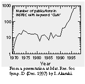
obi: So this period of research certainly seems to have been the source of the current worldwide interest in this field (see figure). But now let's move on to talk about science and education more generally. Do you have any thoughts about how to encourage youngsters to take a greater interest in science and engineering?
Professor Akasaki: I think that young people today have too few occasions to touch and handle the actual working parts of machines, modern electronic gadgets and so on. When I was a young researcher, I used to build my own annealing ovens and furnaces, solder all my electrical contacts manually - I had very little equipment that was automated. Hands-on interactions with that kind of technology is exciting and educational. It continually brings surprises and new discoveries on a very personal level - it stimulates the mind and creates an interest in science and engineering.
These days, though, most equipment for characterisation in universities and industry is highly automated. So students aren't encouraged to think much about its internal workings... It's like using an electronic calculator to give you an answer without your really having to think about how it was derived. My real concern is that "educators" may themselves reach the stage where they do not know enough about the internal workings of devices, machines and so on. We may pay an unexpectedly high price for all the conveniences of the modern age.
obi: We are approaching the 21st century. In your opinion, what idea or discovery has had the greatest influence in shaping our lives in the 20th century?
Professor Akasaki: I think the 20th century was truly the century of "electronics": telecommunications technology, especially, has advanced at a tremendous rate. In the early days we were dependent on vacuum tube technology but in the 1950's the vacuum tube was replaced by solid state devices. Semiconductor technology now governs our daily lives.
obi: Then what about the 21st century?
Professor Akasaki: That is a difficult question! It may be fashionable to say "biotechnology" and such-like, but I do not believe that electronics will give up its dominant position for a very long time to come.
obi: Finally, Professor Akasaki, do you have time to pursue any hobbies?
Professor Akasaki: I enjoy "conversation". I think it is important to talk - opportunities for discussing things with people from a wide range of backgrounds and opinions are not so frequent in this country. I always encourage my students to hold discussions, not just about their research but ranging much wider, over topics such as art, music and history.
My other, more serious pastime is listening to classical music using
amplifiers that I have built myself from vacuum tubes.
I also design and build my own speaker systems-
the biggest "woofer box" I have is about 1.5 metres high.
My hobby makes moving house very difficult!
Interview by Adarsh Sandhu

 ryoku
ryoku
 z
z
